Simulation of Thin Water Layers on Wafer Surfaces During Bond Chamber Evacuation
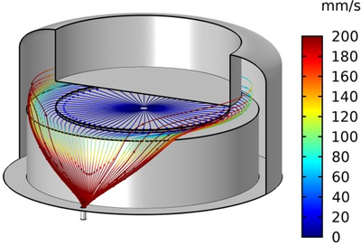
Thin liquid layers play a crucial role in many applications. In the case of direct wafer bonding, the amount of water in the bonding interface determines the bonding strength and is therefore of high interest. Simulations can help to study the influence of different technological and ambient parameters on the water layer thickness on wafers at each process step from wafer pre-treatments to the moment before bonding in an evacuated bond chamber. We combine simple physics-based and literature-known models to simulate this whole process [1]. Spin drying of the wafers after rinsing is described as a balance of viscous and centrifugal forces [2]. The evaporation during the transport of the wafers to the bond chamber is modeled based on the diffusion equation and a mass balance at the water-air interface [3]. With this kind of modeling, it is possible to reduce the need for expensive and time-consuming experiments and, hence, save costs. One important step in the technological process of direct wafer bonding described above is the evacuation of the bond chamber. In the continuum flow regime we use the Laminar Flow interface provided by the COMSOL Multiphysics® software to simulate the gas flow in the chamber. The model describing the evaporation of the water from the wafer surfaces is implemented as a boundary condition using the PDE (Partial Differential Equation) as well as the ODE (Ordinary Differential Equation) and DAE (Differential-Algebraic Equation) interfaces. A pressure curve describing the pump-down of the chamber is used as boundary condition for the flow. As this pressure decreases the Knudsen number (ratio of mean free path of the molecules to a critical system length, e.g., the gap between the wafers) increases. At some point the flow is no longer in the continuum flow regime but in the transitional flow and free molecular flow regime, respectively. For these parts of the pump-down process the Molecular Flow Module is used to capture the physics correctly. Using COMSOL Multiphysics® allows to simulate the whole pump-down process from atmosphere to the pressure desired for the direct wafer bonding process. Utilizing different physics interfaces enables the possibility to study the pump-down in all flow regimes from continuum flow at the beginning to free molecular flow at the end. As an outcome of the simulation, we get the water layer thickness on the wafer surfaces during the complete process.
Download
- Huber_4451_presentation.pdf - 1.68MB