In a paper titled “Choosing a Gate Dielectric for Graphene Based Transistors“, the applications of a semiconducting form of graphene are examined. As we have seen before, single-layer graphene is not a semiconductor, it is a zero bandgap conductor (a semimetal). Efforts are well underway to introduce bandgaps to graphene, which would make it semiconducting with a room temperature mobility an order of magnitude higher than silicon. The race is already underway to find applications for such a material once the remaining technical challenges have been overcome. An application of semiconducting graphene is the design of next-generation, fast switching semiconductor metal oxide field effect transistors (MOSFETs).
What Is a MOSFET?
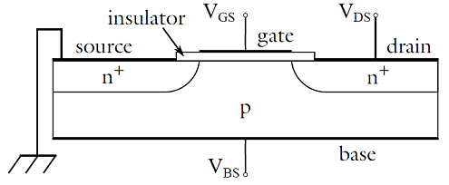
The basic idea of a MOSFET is to apply a gate voltage to control the drain-to-source resistance and thus the drain current (see image below). At a certain gate-to-source voltage (VGS), and at low drain-to-source voltages (VDS), the drain current is almost linearly dependent on VDS. When VDS increases, the drain current saturates. The level of saturation depends on the gate-to-source voltage and the switching time depends on the mobility of the semiconductor. The higher the mobility of the semiconducting material, the faster the current can be switched on and off.

Semiconductor Physics
Semiconductor physics is extremely complicated. Strictly speaking, the Boltzmann equation should be solved with Maxwell’s equations in order to describe the device physics completely. Since this is computationally intractable, the most common approach for modeling semiconductors is to solve a set of drift diffusion equations coupled to Poisson’s equation:
\frac{\partial n}{\partial t}&=\frac{1}{q}\nabla \cdot \mathbf{J_{n}}-R_n \\
\frac{\partial p}{\partial t}&=-\frac{1}{q}\nabla \cdot \mathbf{J_{p}}-R_p \\
\nabla \cdot{} \left(\epsilon \nabla V\right) &= -q(p-n+N_D^+-N_A^-)
\end{aligned}
Here n is the number density of electrons, p is the number density of holes, V is the electrostatic potential, Rn is the electron recombination rate, Rp is the hole recombination rate, Jn is the electron current, Jp is the hole current. Solving this set of equations allows you to construct the voltage-current characteristics of semiconducting devices. The semiconductor equations are highly non-linear and require special numerical methods to solve.
Our Brand New Semiconductor Module
As we recently announced, a dedicated product for modeling semiconductor devices is now available within the COMSOL platform. The Semiconductor Module, as it’s called, allows for detailed analysis of semiconductor device operation at the fundamental physics level. The module is based on the drift-diffusion equations with isothermal or non-isothermal transport models. Two numerical methods are provided: the finite volume method with Scharfetter-Gummel upwinding and a Galerkin least-squares stabilized finite element method. The module provides an easy-to-use interface for analyzing and designing semiconductor devices, greatly simplifying the task of device simulation on the COMSOL platform.
Models for semiconducting and insulating materials in addition to boundary conditions for ohmic contacts, Schottky contacts, and gates are provided as dedicated features within the Semiconductor Module. The module includes enhanced functionality for modeling electrostatics. System level and mixed device simulations are enabled through an interface for electrical circuits with SPICE import capability.
The Semiconductor Module is useful for simulating a range of practical devices. The built-in Model Library contains a suite of models designed to provide straightforward instruction and demonstrate how to use the interface to simulate your own devices. The Semiconductor Module is particularly relevant for simulating transistors including bipolar, metal semiconductor field-effect transistors (MESFETs), metal-oxide-semiconductor field-effect transistors (MOSFETs), Schottky diodes, and P-N junctions.
![]()
The Semiconductor Module could hence be used to investigate the device characteristics of graphene-based semiconductors similar to the ones explained in the paper referenced at the beginning of this blog post.
This Concludes the Graphene Series…
Over the past few months, in the previous four posts of our blog series, we have read lots about the history, applications, and manufacture of graphene. I’ve enjoyed talking about this topic very much — but I’ve only scratched the surface. There are still many sub-topics that haven’t been explored, and I encourage you to keep up with the latest graphene-related developments in technical magazines and publications. Whether you’re interested in the applications or the manufacture of graphene, COMSOL offers a wide range of products that can provide insight and a better understanding of these processes.


Comments (2)
Md. Nahid Hossain
July 6, 2013I want to Design Graphene FET. I want to measure I-V characteristics,capacitance,charge and some device physics phenomena.
I have already tried but not realizing how to measure these characteristics and physics such as electrical potential,Vg & Vds application .
Melina Melina
April 28, 2018How can i model Graphene in semiconductor module?