

When designing products on the nanometer scale, physics interactions that are considered negligible on the larger scale make their presence known. One such case where these forces must be taken into account is in the design of integrated circuits, where understanding and optimizing the effects of van der Waals forces, attractive forces, and surface tension become vitally important to creating a robust design. As technological advancements call for both the size of integrated circuits to decrease and the density of their transistors to increase, controlling the way these forces interact on the nanometer scale is becoming a more and more important task. In order to overcome these new design challenges, researchers at Tokyo Electron America are using simulation to understand and optimize the effect these forces have on integrated circuit features.
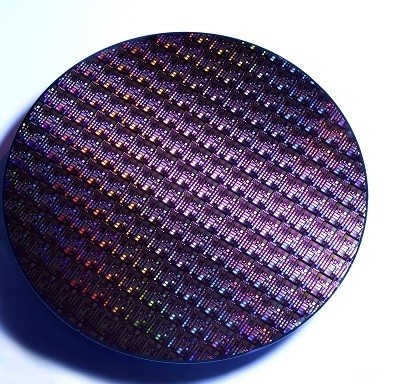
A 300 mm semiconductor wafer patterned using multiple photolithography steps.
The Photolithography Process
The process used for manufacturing integrated circuits is called photolithography, and it involves the etching of a semiconductor wafer on which an integrated circuit is developed. The etching process uses a series of chemical treatments and subsequent cleaning cycles to etch patterns into the surface of a silicon wafer, known as integrated circuit features or nodes.
When integrated circuits are manufactured, it is important to optimize both the pattern development and cleaning processes in order to ensure the success of the design. This is because of the interactions that occur between the cleaning agents and the features defining the patterns, which can ruin the integrated circuit by causing permanent feature deformations. Preventing these deformations is becoming an increasingly difficult task, because as both the size of the features and the spacing between the features decrease, the forces acting on them become even more significant. If these forces cause the features to touch, the integrated circuit can undergo pattern collapse, where the feature shape is permanently bent, pattern integrity is lost, and the integrated circuit is no longer functional.
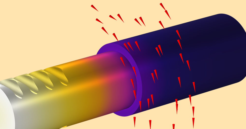
Unwanted mechanical stresses can be introduced through van der Waals attraction forces, as well as through the surface tension due to cleaning fluid trapped between features (shown below). These forces can cause the features to bend inward, and if the features don’t return to their original shape, pattern collapse occurs.

The surface tension force (F) due to the cleaning fluid trapped between the two features. Pattern collapse occurs if the features don’t return to their original configuration and remain touching.
As integrated circuits become smaller, features are also becoming thinner and taller to accommodate the shrinking surface area of the chip, a trend known as node shrink. This trend causes designing and cleaning features to become even more challenging, since the forces acting on the features happen on such a small scale and it is much harder to reach between thin, tall features to remove the cleaning fluid.
Optimizing Integrated Circuit Design
Tokyo Electron America (TEL) develops tools for the manufacturing of integrated circuits using finite element analysis (FEA). In a previous blog post, “Stick a TV to the Wall Using Gecko Feet”, my colleague Phil described an instance in which the van der Waals forces exerted by gecko feet were harnessed and amplified to create a “tape” called Geckskin™ that is capable of holding a TV to a wall. These researchers used van der Waals forces to their advantage, and they were a vital component in producing the final Geckskin™ design. The aim of TEL researchers, however, is to do just the opposite — they are using FEA to find an integrated circuit design capable of withstanding the van der Waals forces exerted on the features, thus minimizing pattern collapse.
The article “Pushing the Limits of Chip Density” from the IEEE Spectrum insert, Multiphysics Simulation, describes how researchers at TEL used simulation software to optimize the design of integrated circuit features. Using COMSOL Multiphysics, TEL researchers were able to optimize the aspect ratio of the features — i.e. the ratio of the feature’s height to its thickness. TEL researchers created a COMSOL model to help them determine which materials and geometric parameters will give rise to pattern collapse, and which will create a stable design. Turn to page 29 in Multiphysics Simulation to read about how TEL researchers were able to successfully utilize simulation to verify and optimize a wide variety of integrated circuit parameters.
Further Reading
- “Pushing the Limits of Chip Density”
- Modeling and Prediction of Line Pattern Collapse, presented at the COMSOL Conference 2012

Comments (0)