

Thanks to the Semiconductor Module and the Application Builder, developing custom optoelectronic simulation apps has never been easier. In this blog post, we show you how to turn a model of an LED device into a user-friendly application that can be used to assess the impact of different designs on the LED’s emission characteristics and performance. We also demonstrate the use of custom methods to manipulate the solution data, enabling the easy creation of bespoke analysis tools.
The Power of Custom Semiconductor Applications
When first introduced in COMSOL Multiphysics version 5.0, the Application Builder marked a shift in the simulation industry, widening its scope with easy-to-use, customized apps based on models. The recently released COMSOL Multiphysics version 5.1 introduced dramatic improvements to this revolutionary tool, enhancing the simulation experience for you — the creator of the app — as well as those using it.
Applications are designed to seamlessly interact with their underlying model to enable dynamic variation of the model parameters as well as the highly customized visualization of model results. This opens up endless possibilities for easily implementing advanced functionality. Such an approach is particularly useful for semiconductor simulations, where an intricate analysis of the solution results is often desired.
We will begin by introducing the InGaN/AlGaN Double Heterostructure LED tutorial model and then demonstrate how to turn this model into an app suitable for designing LEDs to emit within a specified wavelength range. The advantage of building an app is that it takes the advanced physics functionality behind the model and makes it available in a user-friendly interface. A single technical expert can create a complicated finite element or finite volume simulation tool and deploy it to individuals within the design staff who may not otherwise have access to or knowledge of advanced simulation and numerical analysis techniques.
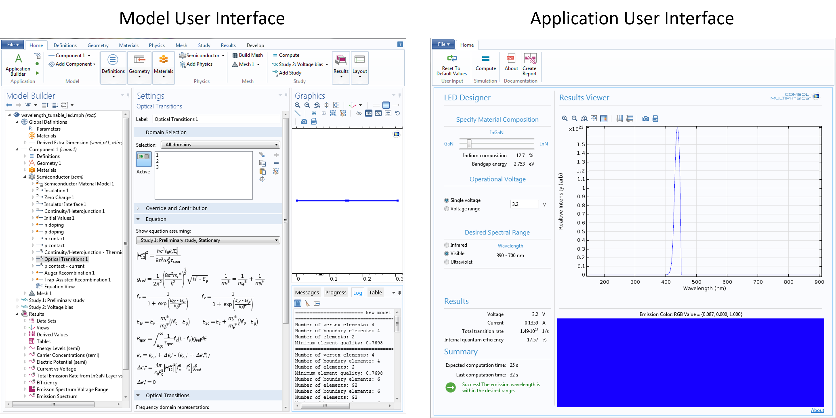
Left: The user interface (UI) of the underlying model shows all of the physics features and the geometry of the device. Right: The application’s UI. While the app has access to all of the model’s physics features, only the settings that need to be varied to enhance the design of the output wavelength are made available. This app offers a much simpler UI without compromising performance.
The Ins and Outs of “Appification”
As mentioned above, applications utilize all of the same physics from the underlying model, while benefiting from a more intuitive user interface and results display. Although the performance and accuracy of the simulation are not affected, the compromise for this increased usability is that apps are less versatile than the models they are based on. Apps should be carefully created for a specific purpose and present users with only the functionality that is needed to satisfy their design requirements.
The Wavelength Tunable LED demo app can be used to assess the emission properties of a AlGaN/InGaN light-emitting diode in order to assist in the design of LEDs that emit within a user-specified wavelength range. The process of converting the InGaN/AlGaN Double Heterostructure LED tutorial model into an app as well as more general tips and tricks for making your own semiconductor applications are discussed in detail here.
From the previous screenshot, it is clear that the required functionality for simulating a wavelength tunable LED has been made available through utilizing several different “panels”. For example, the Specify Material Composition, Operation Voltage, and Desired Spectral Range panels enable input design decisions about the LED device, with results displayed in tabular and graphical forms in the Results and Results Viewer panels, respectively.
Additionally, the material properties of the LED can be varied as well as the voltage applied to the device, and the app calculates the emission intensity, electroluminescence spectrum, and device efficiency. The emission spectrum is analyzed to determine if the emission falls within the desired spectral range. If the app is used to design an LED that emits in the visible spectrum, the electroluminescence is converted into an RGB color ratio and displayed to provide immediate feedback on the emission color of the device.
InGaN/AlGaN LEDs: The Physics Behind Emission Color
When designing an application, you have to consider which physics features need to be accessible and how to link the important physics principles to your app’s UI. For example, in the Wavelength Tunable LED app, modification of the emission wavelength is necessary. As the emission wavelength from semiconductors is highly dependent on the bandgap energy, this is achieved by allowing the material composition of the LED to be varied.
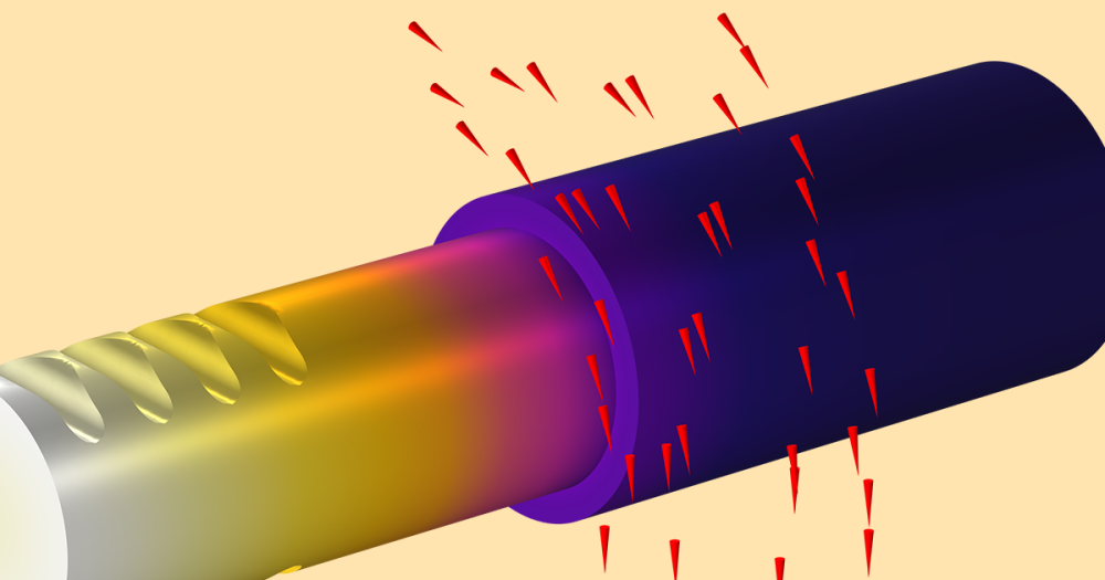
The active region of the LED from which light is emitted is made of InGaN, which is a semiconductor alloy comprised of indium nitride and gallium nitride. Indium nitride has a small bandgap of around 0.75 eV and emits infrared light; gallium nitride has a much larger bandgap (approximately 3.4 eV) and emits in the far ultraviolet range. By varying the blend of the InGaN, it is possible to create a material that emits between these two extremes, thus any color of visible light is possible.
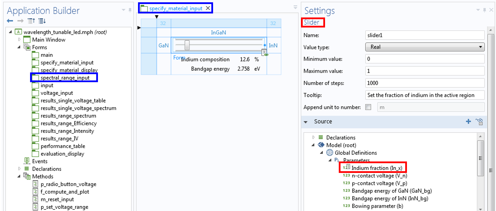
The slider settings in the Application Builder. It is straightforward to link a graphical input, such as the slider bar, to a model parameter. In this case, the slider bar is used to set the fraction of indium in the InGaN alloy.
The fraction of indium in the active region material can be varied using an interactive slider bar within the Specify Material Composition panel of the Application window. The slider bar is linked to a parameter, In_x, in the underlying model that is used to set the fraction of indium in the InGaN material. When the slider is moved, the value of In_x is automatically varied between the minimum value and the maximum value (shown under the settings for the slider). The value of In_x is then used “behind the scenes” to calculate the bandgap energy for the InGaN material used in the light-emitting region of the device.
The app provides dynamic feedback by updating the indium composition and bandgap energy displays in real time as the slider is changed. The screenshot below shows how two data displays, one for each value, are used to achieve this. Each data display is linked to a parameter that is calculated using the value in In_x. When the slider is moved, the data display automatically updates to indicate the new corresponding values.
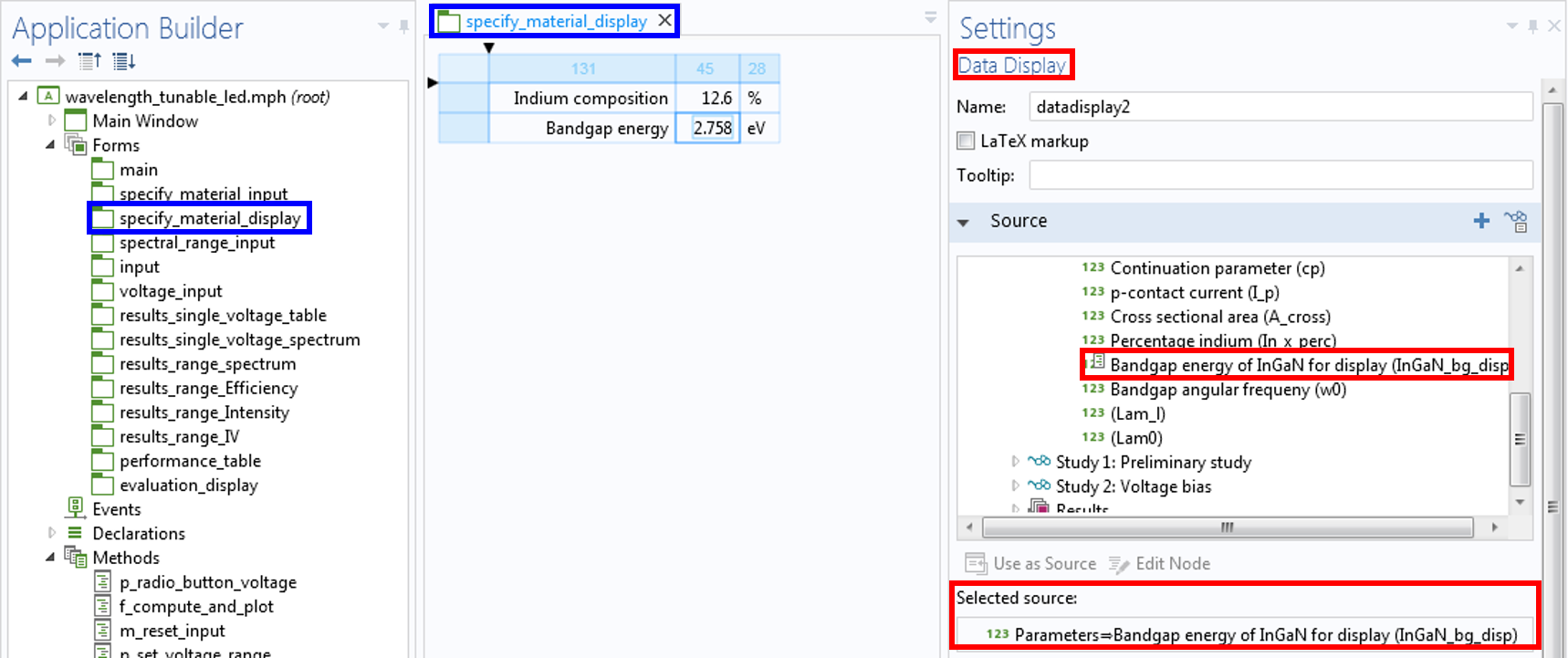
Settings for the bandgap energy data display. It is straightforward to link a data display with any model parameter. Here, the data display is linked to the parameter that represents the bandgap energy of the InGaN material.
Using a similar approach, the input box for the operational voltage is linked to a model parameter. The voltage that is applied across the LED can be set. In general, it is good practice to create models where the user-controlled variables are accessible via parameters, as this is the easiest way for others involved in the design process to interact with them through apps. For semiconductor simulations, quantities required by the physics features are often functions of several user inputs, and it is important to carefully consider which inputs should be included in the UI.
Automating Results Analysis Techniques Through Custom Methods
In addition to offering a simplified user interface, applications also allow custom methods to be created. Custom methods are extremely powerful and can be used to automate any of the functionality in COMSOL Multiphysics. They can also be used to manipulate solution data to perform an analysis in order to extract important figures of merit. This is particularly significant for semiconductor devices, where the device operation can often be evaluated by extracting device-specific values, such as turn-on voltage for a MOSFET transistor or the current gain for a bipolar transistor.
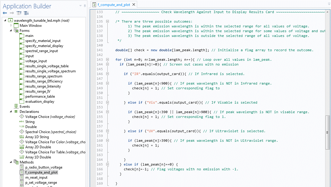
In this app, a custom method is used to analyze the emission spectrum from the LED. The wavelength of peak emission is extracted from the spectrum and compared to the selection in the Desired Spectral Range panel. This panel contains a button that enables the selection of either infrared, visible, or ultraviolet as the spectral desired emission range and a dynamic feedback that displays the corresponding wavelength range. The screenshot below shows the settings window for the radio button. The radio button is configured by linking it to a choice list, which, in this case, contains the three spectral options for selection as well as a source variable in the declarations. The source variable is used to set the initial value of the radio button. When the radio button is modified, the corresponding value is written into the source variable.
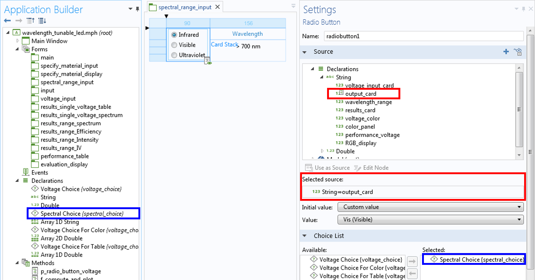
The configuration of the radio button from the Desired Spectral Range panel. The blue boxes highlight the selected choice list, which contains the three possible options. The red boxes indicate the output_card variable, which is used as a source for the button. This variable holds a value that corresponds to the radio button’s selected option.
The source variable — in this case, output_card — can then be used within custom methods. The following screenshot shows an example section of the custom method f_compute_and_plot. This method is executed by clicking the Compute button in the ribbon and solves the underlying model by using the current input settings and performing an analysis of the results. The section depicted in the screenshot compares the wavelength of emission to the radio button selection stored in output_card. If the peak emission wavelength falls within the selected spectral range, a flag variable, check[n], is set to 1. The flag variable is later used to control the message displayed in the Summary section that indicates whether the desired emission wavelength has been achieved.
A section of the f_compute_and_plot custom method that evaluates if the peak emission wavelength falls within the selected desired spectral range.
We have just demonstrated how a user-specified input and a value extracted from a solution can be combined with a custom method to implement highly flexible functionality within the application. The radio button within the Operation Voltage panel is used similarly in other logical conditions that control which analysis to perform on the solution. When a single voltage is selected, only the emission spectrum is plotted as a graph. However, when a voltage range is selected, the other performance metrics from the Results panel are also plotted as a function of voltage.
In addition to performing logic operations, you can also use custom methods to execute Java® code to perform a more complicated analysis of the results. The screenshot below shows a private method — nested within the f_compute_and_plot method — that converts the emission spectrum into an RGB value. Each color component is obtained by multiplying the spectrum by the corresponding color sensitivity curve and integrating it with respect to the wavelength. You can explore this in further detail within the application by clicking the About button.
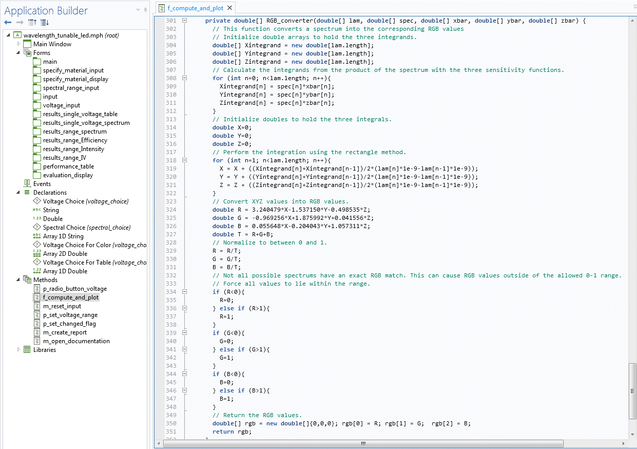
The RGB_converter() method. This is a private method within the f_compute_and_plot method that is used to convert the electroluminescence spectrum into an approximate RGB value to display the emission color if it falls within the visible range. It is an example of how custom functionality can be implemented using methods.
With this example, we can see how advanced operations can be performed on solution data to create custom displays or feedback within applications. The screenshot below shows the app after solving for two different values of the indium composition. InGaN with 12.7% indium emits blue light; InGaN with 23.7% indium emits green light. This offers immediate feedback from the app when designing an LED for visible emission.
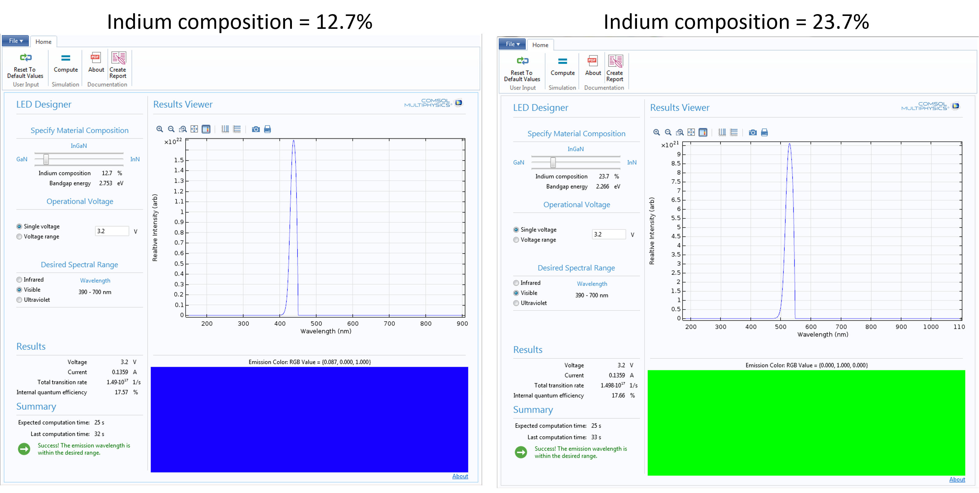
A screenshot of the app after solving with two different slider bar positions. The left image represents the default case of 12.7% indium composition. The right image illustrates an increased indium composition of 23.7%.
Documenting Apps for Usability
To ensure that your application can be used effectively, it is often a good idea to document your app. This can easily be done by utilizing an embedded file that is linked to a button, such that it can be opened with a single click (shown in the screenshot below). Here, you can include a summary of the physics behind your semiconductor simulation along with some instructions on your app’s purpose and how it should be used. COMSOL includes a Report Generator feature, which can be used to create your documentation. You might also consider implementing tooltips on buttons and user input fields to provide more immediate help to those using your app.
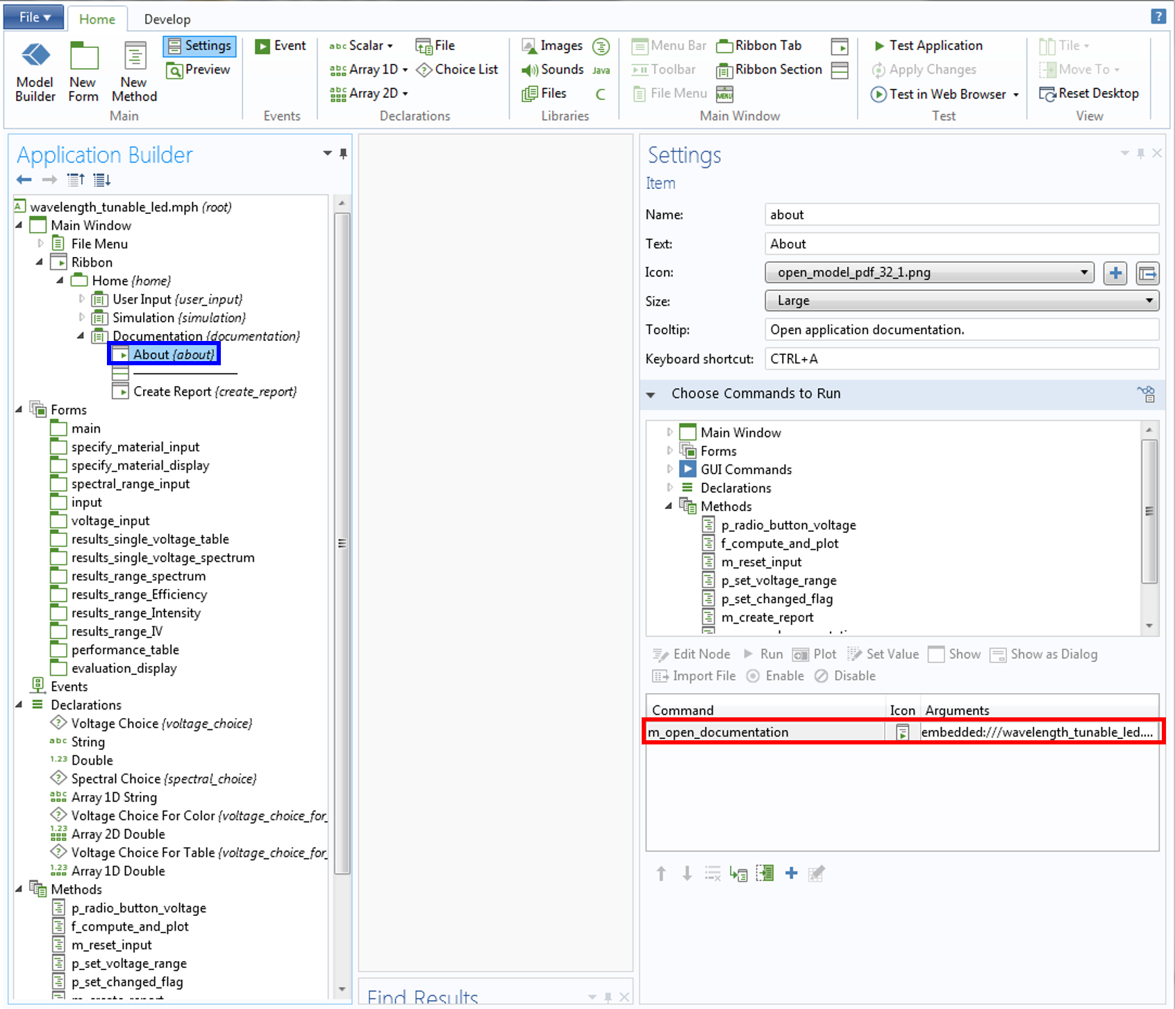
The settings window for the About button in the application ribbon. The button is set to open the embedded PDF file that contains the app’s documentation. The text in the tooltip input field is displayed when the cursor hovers over the About button.
Best Practices for Creating Apps
Before you begin designing your own app, it is helpful to ask yourself the following questions:
- What is the purpose of the application?
- Apps work best when they are designed to address specific simulation goals.
- What physics features does the application need to have access to?
- Try to parameterize any variables that the app needs to modify.
- How should the user interface be structured?
- Try to present only necessary functionality. Consider using panels in the layout for user inputs and selections.
- How should the user interact with variables?
- Slider bars work well when a quantity varies between two known limits.
- Radio buttons are helpful in making selections among several predefined options.
- Input boxes can be used to allow custom values to be entered.
- What results need to be displayed to provide the required feedback?
- Graphs, tables, or display boxes are suitable for displaying simulation results.
- Can custom methods be used to enhance the functionality of the application?
- Use custom methods to perform a bespoke analysis on the solution data, if required.
- What documentation is required in order for the application to be used effectively?
- Documents can be embedded inside application files. Include PDF instructions on how to use your app along with a brief explanation of the physics involved.
Considering these questions will help you maximize the usability of your app and create powerful tools for performing semiconductor simulations. COMSOL Multiphysics version 5.1 makes it easy to quickly package advanced semiconductor simulations into easy-to-use analysis tools that can be used by those who are not experts in simulation to optimize the design of the device.
Additional Resources
Oracle and Java are registered trademarks of Oracle and/or its affiliates.


Comments (0)