Pushing the Limits of Chip Density
Derek Bassett and Michael CarcasiTokyo Electron America
Austin, TX
Chip manufacturers have been adhering to Moore’s law, a law stating that the number of transistors that can be economically placed on an integrated circuit doubles every year, since 1965. As the number of transistors increases, however, the process of manufacturing integrated circuit, called photolithography, becomes more difficult. Each device requires approximately 200 cleaning and photolithography steps and any failures in this process can cost millions.
Tokyo Electron America (TEL), a producer of manufacturing tools vital to the processing of integrated circuits, used simulation to understand a type of failure called pattern collapse. Pattern collapse occurs when cleaning fluid between two features evaporates and the changing surface tension occurring during the evaporation causes the features to bend. Ideally, those features return to their normal shape, but sometimes they are permanently deformed.
Using COMSOL Multiphysics, researchers at TEL created a 2D structural mechanics model based on a series of steady-state calculations with the surface tension forces as boundary conditions. They compared those results with experimental data from literature and found that the model accurately predicted the critical aspect ratio for collapse.
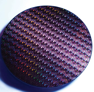 300mm semiconductor wafer patterned using multiple photolithography steps.
Download
- Tokyo_Electron_MS2013.pdf - 2.51MB